I tutorial di EO-WEB (capitolo 2) – Signal Chain Processing. Analog Front End: Variable Gain Amplifiers

Dalla rivista:
Elettronica Oggi
Another widely used, low cost solution is to obtain the same functionality of the PGA using opamps in the inverting or non-inverting configuration, where the gain resistors can be chosen within a set with an analog switch (Fig. 1)
Although this is probably the easiest circuit that can be devised, it also has many drawbacks for which its use in real applications should be very carefully considered.
Apart from the problem already encountered for PGAs – available gains are few and can only be changed in finite steps – the use of external resistors gives two major problems:
1. resistors should be “good”, that is they should have low tolerance
2. they are sources of noise.
The input/output relationship for the circuit in figure 1 is:
![]()
eq. 1
.jpg)
Fig. 1 – Variable Gain Amplifier: operational amplifier implementation
The error due to resistance value tolerance (1% or 2% in this example) is computed in the following
Table 1 (see Excel file: Gain Error)
where Gain+- , for instance means:
![]()
eq. 2
where, in case of 1% tolerance
![]()
eq. 3
and
![]()
eq. 4
As far as tolerance is concerned, a 1 % tolerance on resistors (with for instance R1 = 1K.W and Rf = 99K.W, G =100) gives origin at most to a 2% error on the gain.
As for noise, remembering that the noise generated by a resistor is
![]()
eq. 5
the highest gains also bring the highest noise voltage, because of the high value of Rf.
The noise equation above describes one of the many noise sources: it is called thermal noise because it is caused by the movement of electrons in resistor. From physics, this noise is directly related to the resistor temperature: its value (T, in degree Kelvin) is in fact present in the equation.
Another problem which is usually disregarded in the use of analog switches is that they present a resistance (RDS ON) which can widely vary according to the manufacturer; this resistance may also differ from channel to channel inside the same chip. These changes can be up to 10% or 20% of the “ON” resistance, and in precision measurement this could be a problem.
In high precision measurement and when the sensors present relatively high impedance, care must be taken in the choice of the topology of the amplifier, so that the measurement circuit presents a low load (high impedance) to the sensors themselves.
Analog Front End: Reference Voltage
A final issue, often understated in designing low cost acquisition systems is the choice of the correct reference voltage source, which essentially depends on the desired accuracy. In most solutions the reference voltage input of Analog to Digital converters or biasing circuits is directly connected to the Vcc rail, obtained with a cheap regulator. In these systems, since the regulated voltage is supplied both to the digital and analog parts of the circuit, specific care should be taken in filtering the ripple induced by switching digital gates into the supply rails.
In more accurate systems, reference voltage is obtained with dedicated chips. The reference voltage determines the full scale voltage of the converter that is the LSB width. The main specs that must be carefully analyzed are nominal output voltage and its guaranteed range, line regulation, noise and output voltage drift. Table 2 summarizes these values for a very common, low cost voltage regulator and for a specific voltage reference chip.
Table 2
The digital approach
From this section on, the digital approach to the problem of processing field data is addressed. The signal chain (in the digital world) of figure 2 will be considered. Each block will be investigated in details, focusing on its performances and what designers should be aware of.
.jpg)
Fig. 2 – Signal Chain: the Digital Approach
A high degree of cause-effect relationship is present in such systems, so that often the reason for some choices in a block depends on blocks that follow in the chain. Thus the reader is suggested to read once all the following sections to get a generic understanding, even if not everything is completely clear at first glance. Then the reader is invited to go back and read again with attention each section: interconnection should at that time be clearer.
The logic order of the operations as implemented in a real system is correctly shown in figure 2. However, for clarity reasons, the Analog to Digital Converter block will be introduced before the low-pass filter in the first block. The reason for this stems from the fact that the low-pass filter has to be used as a consequence of the presence of the Analog to Digital Converter itself.
Digital Signal Processing
Signals from the field can be processed either in the analog domain or in the digital domain; it should however be understood that some kind of analog processing is always needed also in a digital system.
The use of digital signal processing allows the implementation of some techniques that are completely new and different from what is available in analog. Versatility, easy of change and age independency are among the most relevant advantages of a digital solution. Of course nothing comes for free. Some key concepts must be very clearly understood by those designers who are willing to use the powerful digital signal processing techniques for their designs. Misinterpretation of the basic rules of digital signal processing may easily bring to wrong and completely unexpected results.
Thus the world of digital processing will be investigated with some details. What follows is not intended as a theoretically precise lesson on Digital Signal Processing. Although at the author’s knowledge every part is correct, some sections may seem too simple/banal to theory experts. The main goal of this article is to supply the reader with some basic tools he can use to understand digital processing and to effectively use the results in a real project.
In following sections very few equations and formula are presented. The author’s intention is that all sections should be read and understood without the need of any use of paper and pencil. As a consequence references to the results of computations will only be presented with some basic explanations to allow readers to use them. Interested readers can refer to Appendixes where all results are explained in details and the equations to justify them are derived. Vey often some additional info is also provided.
Taking into consideration a typical system operating in the real world, the sequence of operations required in a traditional sampled signal system (digital
system) is considered. As shown in fig. 2 the input signal [s(t)] is processed by the following blocks:
1. Low pass filter (anti-alias filter). It is used to remove the unwanted spectral components of the input signal; the frequency where it reaches its maximum attenuation is named fm. Some additional analog processing may be required depending on the application. In this case some of the considerations presented in previous paragraphs will still be valid and apply.
2. Analog to Digital Converter: it transforms the analog input signal [x(t)] into a digital word [x(n)] that represents its value.
3. Digital Signal Processor. This is the processing unit that performs the specific required task. It can be a microprocessor, microcontroller or digital signal processor or any other chip capable of number crunching.
4. Digital to Analog Converter: in many real systems, the result of the digital processing is applied back to the field. This requires the digital word [y(n)], result of the computations, to be converted back into an analog signal [y(t)].
5. Analog low pass filter (reconstruction filter): used to remove unwanted spectral components of the processed signal to get the output signal [z(t)].
Table 3 – Here below summarizes the signals, domains and characteristics of the signals involved in the chain just described
(*) this is true as far as the Digital to Analog Converter operation itself is considered. The real analog value will be different from the theoretical value because of component tolerances, temperature, time
Excel File: Gain Error
This spreadsheet computes the real gain that can be obtained by the circuit of figure 1 when taking into consideration resistors tolerance.
The user can edit the columns titled Tolerance, R1 nom and Rf nom (green bold). All other values are computed.
Here below the equations used in the spreadsheet:
![]()
eq. Excel 1
![]()
eq. Excel 2
![]()
eq. Excel 3
![]()
eq. Excel 4
![]()
eq. Excel 5
![]()
eq. Excel 6
![]()
eq. Excel 7
Queequeg2004
Contenuti correlati
-
Difesa e Aerospazio; il ruolo degli amplificatori di potenza
Grazie ai PA MMIC in nitruro di gallio è possibile affrontare in maniera efficace le complesse problematiche legate alla realizzazione di sistemi per comunicazioni satellitari militari, radar e 5G Leggi l’articolo completo su EO 514
-
I componenti necessari per la ricarica efficiente dei veicoli elettrici
Si trova in ogni veicolo all-electric e determina spesso il tempo di ricarica alla colonnina di ricarica AC: si tratta del caricatore di bordo (OBC). Per renderlo compatto, leggero, efficiente e silenzioso, sono necessari componenti ad alte...
-
Controllo sinusoidale senza MCU di motori sincroni a magneti permanenti
Grazie alla disponibilità di circuiti integrati come il pre-driver a onda sinusoidale TC78B011FTG di Toshiba, è possibile eliminare il ricorso a un microcontrollore per il controllo “sensorless” dei motori brushless Leggi l’articolo completo su EO 511
-
Garantire una protezione dei circuiti compatta, flessibile e precisa
Per implementare rapidamente funzioni di protezione compatte e precise, conformi agli standard di sicurezza UL e IEC, i progettisti possono ricorrere ai regolatori eFuse, circuiti integrati di protezione dotati di soglie di protezione programmabili in grado di...
-
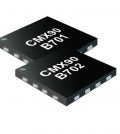
CML Microcircuits amplia la famiglia di prodotti SµRF
CML Microcircuits ha annunciato la disponibilità degli amplificatori con curva di guadagno a pendenza positiva CMX90B701 e CMX90B702. Questi dispositivi costituiscono le ultime aggiunte alla famiglia di prodotti SµRF di CML e proseguono l’espansione di CML verso...
-
Progettazione di asset tracker low power: importanza dei componenti analogici e della gestione dell’alimentazione
Questo articolo esaminerà le problematiche tecniche che devono affrontare i progettisti durante lo sviluppo dei tracker wireless: l’accento è posto sulla scelta dei componenti analogici e sui vincoli imposti dal funzionamento a batteria Leggi l’articolo completo su...
-
La progettazione analogica entra nell’era digitale grazie ai tool di nuova generazione
Tool hardware e software innovativi stimoleranno l’interesse dei giovani ingegneri verso il mondo dell’analogica Leggi l’articolo completo su EO 503
-
AFE per il monitoraggio dei parametri vitali per uso clinico
Il nuovo MAX 86178 di Analog Devices integra tre sensori – PPG, ECG e BioZ in un unico package, grazie ai quali è possibile rilevare l’insorgere di una malattia prima del manifestarsi dei sintomi Leggi l’articolo completo su EO 499...
-
Progettazione con amplificatori operazionali a bassa potenza: tecniche di risparmio energetico per circuiti ad amplificatore operazionale (1° parte)
Negli ultimi anni, la diffusione dell’elettronica con alimentazione a batteria ha reso il consumo energetico una priorità crescente per i progettisti di circuiti analogici. Tenendo in considerazione questo aspetto, questo articolo è il primo di una serie...
-
Circuiti integrati a segnali misti: tra analogico e digitale
Telefonia mobile, IoT e automotive sono i principali propulsori della domanda di circuiti analogici, digitali e a segnali misti con caratteristiche di basso consumo e ingombro ridotto Leggi l’articolo completo su EO 499


