7 fellows & 7 thoughts about Moore’s Law – “We must teach chips to feel pain”
-

- Tweet
- Pin It
- Condividi per email
-

When I was a doctorate student in the 1980s there was lots of wild speculation about Moore’s Law: give it another 10 years and transistors will stop getting smaller, they were saying back then. But in the end, the creativity of engineers turned out to be greater than the pessimism of the forecasters.
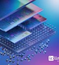
Yet today I believe that we are close to the end of Moore’s Law. Increasingly fewer companies are now manufacturing chips, because it is becoming too expensive and too complex. It is a race of elimination that will gradually see Moore’s Law extinguished. And, of course, we are also virtually at the limits of the physical boundaries involved. Transistors today are just a few dozen atoms in length. And you can’t make things smaller than one atom.
In actual fact, Moore’s Law ceased some time ago to be driven purely by making the dimensions of transistors smaller. More and more, gains in performance are coming from the introduction of new materials (first for interconnects and gate dielectrics, and now also for the transistor channel itself). This is done by replacing planar by 3D MOSFET transistor architectures, while in the future we will even see MOSFETs being replaced by alternative concepts such as tunnelFETs, carbon nanotubes or spin wave devices.
However, this last technology will have enormous implications for chip designers. When that happens, the whole ecosystem built around the MOSFET, with models, simulation tools, libraries, etc. will have to be replaced or adapted significantly. The question is whether the investment, effort and risk involved with upsetting this whole ecosystem may outweigh the benefits of such a switch.
In the area of the reliability of chips, there are enormous challenges ahead if we abandon the tried-and-tested MOSFET transistor. First and foremost, if we introduce new materials and designs for our devices, we will have to embark on a learning curve in which we will need to understand any new failure mechanisms that come along. For the classic MOSFET, that means a learning curve of 50 years.
But if we introduce new concepts, we will have to start virtually back at zero again. Also in the future we will probably not be able to guarantee that all of a chip’s transistors will continue to operate reliably throughout the whole proposed service life. Unless we approach the whole thing differently, that is. Design, device and technology engineers will have to work much more intensively together to ensure a reliable system, even if it is built using transistors that are not 100% reliable.
Research into this is already underway at imec. If we use innovative design methodologies that detect and resolve problems during runtime, a reliable system can be achieved. This can be compared with the human body feeling pain when something is wrong. So we need to teach transistors to feel ‘pain’ so that we can adjust the parameters at runtime and make the system continue to keep working that way. This means that innovation will no longer mainly come from the technology, but from smart design and carefully considered applications. It promises to be a major challenge!
About the author
Guido Groeseneken received the M.Sc. degree in electrical and mechanical engineering (1980) and the Ph.D degree in applied sciences (1986), both from the KU Leuven, Belgium. In 1987 he joined the R&D Laboratory of IMEC (Interuniversity Microelectronics Center) in Leuven, Belgium, where he is acting as scientific fellow, covering research fields of advanced devices and reliability physics of Sub 22nm CMOS technologies. Since 2014 he is also responsible for the academic relations of imec with universities worldwide. Until 2014 he was managing the device reliability group. From October 2005 until April 2007 he was responsible for the IMEC Post CMOS Nanotechnology program within IMEC’s core partner research program. Since 2001 he is Professor at the KU Leuven, where he is managing a European Erasmus Mundus Master program in Nanoscience and nanotechnology. Since January 2005 he is elected to the grade of IEEE Fellow
He has made contributions to the fields of non-volatile semiconductor memory devices and technology, reliability physics of VLSI-technology, hot carrier effects in MOSFET’s, time-dependent dielectric breakdown of oxides, Negative-Bias-Temperature Instability effects, ESD-protection and –testing, plasma processing induced damage, electrical characterization of semiconductors and characterization and reliability of high k dielectrics. Recently he has also interest in nanotechnology for post-CMOS applications, such as carbon nanotubes for interconnect and sensor applications, tunnel FET’s for alternative ultra-low power devices etc.
He has served as a technical program committee member of several international scientific conferences, among which the IEEE International Electron Device Meeting (IEDM), the European Solid State Device Research Conference (ESSDERC), the International Reliability Physics Symposium (IRPS), the IEEE Semiconductor Interface Specialists Conference (SISC) and the EOS/ESD Symposium. From 2000 until 2002 he also acted as European Arrangements Chair of IEDM. In 2005 he was the General Chair of the Insulating Films on Semiconductor (INFOS) conference, organized in Leuven, Belgium and in 2008 he co-organized the European ESREF conference in Maastricht, The Netherlands. Finally from 1999 until 2006 he acted as an editor of IEEE Transactions on Electron Devices. Since 2006 he is member of the IEEE EDS Fellow evaluation commission. Since 2012 he is member of the IEEE J.J. Ebers award committee.
Guido Groeseneken, imec fellow and fellow IEEE Electron Devices Society
Contenuti correlati
-
 Nuova tecnologia produttiva da imec e EVG
All’Ieee Electronic Components and Technology Conference (Ectc) 2026, imec ed EV Group (EVG) hanno presentato una tecnologia di bonding ibrido wafer-to-wafer ad alta resa con passo dei pad di interconnessione in rame di 200 nm. Zsolt Tokei,...
-
 IC-Link by imec entra in Tsmc OIP
IC-Link by imec, fornitore di servizi di progettazione e produzione di Asic e fotonica al silicio, è entrato a far parte della Tsmc Open Innovation Platform (OIP) 3DFabric Alliance. Grazie a questa partnership, IC-Link potenzierà le proprie...
-
 Amazon e i chip per l’intelligenza Artificiale
Se l’attività di produzione di chip di Amazon fosse un’azienda a sé stante e vendesse i chip prodotti quest’anno ad AWS e ad altre terze parti, il fatturato annuo si aggirerebbe intorno ai 50 miliardi di dollari....
-
 Qualificazione ELDRS per i transistor JAN di Microchip
Microchip Technology ha annunciato che i suoi transistor JAN (Joint Army Navy) sono stati testati e qualificati per i requisiti dello Standard Militare Enhanced Low Dose Radiation Sensitivity (ELDRS) tra cui MIL-STD-750, Test Method 1019 e specifiche...
-
 Il GaN nella progettazione di alimentatori: vantaggi e sfide
I transistor GaN aprono la strada allo sviluppo di progetti di alimentatori caratterizzati da efficienze più elevate, densità di potenza maggiori e fattori di forma più ridotti Leggi l’articolo completo su EO Power 35
-
 Inova Semiconductors riceve il premio Digital Innovator 2023
Inova Semiconductors è stata nominata “Digital Innovator” per il terzo anno consecutivo dalla rivista di PC Chip insieme agli esperti di Globis Management Consulting. Chip ha condotto un’indagine sulle innovazioni digitali con l’obiettivo di trovare aziende tedesche...
-
 La progettazione dei circuiti elettronici
In questo articolo, dopo l’esposizione dei principi base della progettazione e dell’analisi dei circuiti elettronici, verrà fornita una sintetica descrizione della progettazione elettronica assistita da computer Leggi l’articolo completo su EO 507
-
 Monitoraggio dello stato dei satelliti mediante amplificatori di rilevamento della corrente
Gli amplificatori di rilevamento della corrente costituiscono un elemento fondamentale di numerosi sistemi di monitoraggio dei satelliti che permettono di capire il loro comportamento dalla Terra Leggi l’articolo completo su EO 507
-
 I chip chiave per Industria 4.0
Alcune categorie di circuiti integrati stanno guidando la crescita dei chip dedicati al mondo della Internet of Things. In uno studio sul comparto, la società di ricerca IoT Analytics individua quattro categorie principali: MCU, chip di connettività,...
-
 CEVA celebrates 15 billionth CEVA-powered chip shipped
CEVA announced that cumulative royalty-bearing chip shipments that include CEVA IP surpassed 15 billion units during the second quarter. This significant milestone has been achieved as CEVA approaches it’s 20-year anniversary of being a public company. While...
Scopri le novità scelte per te
-
Nuova tecnologia produttiva da imec e EVG
All’Ieee Electronic Components and Technology Conference (Ectc) 2026, imec ed EV Group (EVG) hanno presentato una tecnologia...
-
IC-Link by imec entra in Tsmc OIP
IC-Link by imec, fornitore di servizi di progettazione e produzione di Asic e fotonica al silicio, è...

News/Analysis Tutti ▶
-
 Cosmic Semiconductor Solutions a Pcim Europe 2026
Cosmic parteciperà per la prima volta a Pcim Europe 2026, evento che si terrà a...
-
 29 premi per DigiKey
In occasione dell’EDS Leadership Summit 2026, evento tenutosi dal 18 al 22 maggio a...
-
 Le previsioni di Wsts sui semiconduttori per il 2026
L’organizzazione World Semiconductor Trade Statistics (Wsts) ha rivisto sensibilmente al rialzo le sue previsioni...
Products Tutti ▶
-
 Soluzione di conformità ASA-ML da Rohde & Schwarz
Rohde & Schwarz ha presentato una nuova soluzione di conformità ASA Motion Link per...
-
 Emerson amplia la gamma NI PXI
Le più recenti aggiunte al portafoglio VST (Vector Signal Transceiver) NI PXI di Emerson...
-
 Microchip presenta una serie di DSC essenziali
Microchip Technology ha introdotto una nuova famiglia di Digital Signal Controller (DSC) che permette...

