Nexperia obtains 100% ownership of Newport Wafer Fab
-

- Tweet
- Pin It
- Condividi per email
-
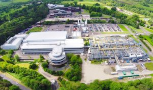
Nexperia has completed the transaction to acquire Newport Wafer Fab (NWF), to be renamed Nexperia Newport, contributing to the company’s growth ambitions and investments to boost global production capacity.
With the acquisition, Nexperia obtains 100% ownership of the Welsh semiconductor production facility. Nexperia Newport will continue to have a strong position in the Welsh ecosystem and technology development and will secure the current jobs at the Newport site and others across the region. Current capacity is over 35,000 200 mm wafer starts per month covering a wide range of semiconductor technologies ranging from MOSFETs and Trench IGBTs using wafer thinning methods to CMOS, analogue and compound semiconductors.
The Newport site complements Nexperia’s other European manufacturing operations in Manchester and Hamburg, which have also seen significant recent investments.
Commented Achim Kempe, Nexperia’s Chief Operations Officer: “We are very excited to include Newport as part of our global manufacturing footprint. Nexperia has ambitious growth plans and adding Newport supports the growing global demand for semiconductors. The Newport facility has a very skilled operational team and has a crucial role to play to ensure continuity of operations. We look forward to building a future together”.
Added Paul James, Operations Director at the Newport site: “The acquisition is great news for the staff here in Newport and the wider business community in the region as Nexperia is providing much-needed investment and stability for the future. We are looking forward to becoming part of the global Nexperia team and are keen to keep the current workforce. Additional local resources may be required too. We are also pleased that we will be able continue to contribute to the local ecosystem.”
Drew Nelson, departing chairman Newport said: “The change in ownership of the Newport site marks an important step for the future of the facility as well as for the region. We are pleased that we are able to maintain the expertise in developing high end silicon devices in the 200 mm wafer fab while at the same time opening up opportunities for us to add new semiconductor technologies”.
Contenuti correlati
News/Analysis read all ▶
-
 Infineon provides FOXESS with power semiconductors
Infineon Technologies supplies its power semiconductor devices to FOXESS, a fast-growing company in the...
-
 Anglia Live expands footprint into Europe
Anglia Components PLC recently announced it is bringing the Anglia Live eCommerce platform to...
-
 Renesas expand its power semiconductor production capacity
Renesas Electronics announced that it has started operations at its Kofu Factory, located in...
Products read all ▶
-
 New SMARC module from Kontron
Kontron expands its existing SMARC portfolio with a module that features the i.MX8M Plus...
-
 New rev of MIKROE ’s NECTO multi-architectural IDE
MIKROE has announced that the latest version of its multi-architectural IDE, NECTO Studio 6.1,...
-
 Neousys debuts new IP66 waterproof computer with Intel 13th/12th-Gen Core
Neousys Technology adds a new series to its waterproof industrial computer family featuring an...

