EDA market – Answers provided by Craig Cochran, Vice President of Marketing, Cadence
-

- Tweet
- Pin It
- Condividi per email
-

EONEWS: What are your opinions regarding the major trends for this market (slowing, growing, booming…)
Cochran: The EDA market is growing at a healthy pace. More significantly, perhaps, the notion of what “EDA” includes will greatly expand in 2015. EDA is no longer just about tools, but is also closely linked with semiconductor IP. EDA is no longer just aimed at individual boards or chips, but at whole systems or end products. And EDA is no longer focused only on hardware, but is increasingly taking embedded software into account.
While “core” EDA is aimed at designing ICs and systems on chip (SoCs), what Cadence calls System Design Enablement (SDE) starts with the end product and the applications (“apps”) it will run. SDE focuses on the design, integration, and verification of chips, boards, packaging, embedded software, and system-level IP. It considers how these components tie into the mechanical and thermal aspects of a system. To support SDE, EDA vendors must provide not just tools but also IP, services, and software content.
The reward for a strong SDE portfolio will be exposure to a far wider market. Systems companies today are undergoing a vertical re-aggregation process in which they are taking more responsibility for hardware and software development – and with worldwide revenues around $2.6 trillion, the systems market is about 10 times larger than the semiconductor market, the traditional focus of EDA. Meanwhile, semiconductor vendors are increasingly called upon to provide software with their chips.
An industry trend called “shift left” will help make SDE possible. With shift left, tasks that were traditionally done later in the design flow occur earlier and in parallel with other tasks. In particular, embedded software can be co-developed and co-optimized with system hardware, rather than tacked on later. Functional verification can be driven by software and based on actual use cases. Another aspect of shift left is an early and close collaboration between foundries, IP providers, and EDA vendors to “co-optimize” tools and IP subsystems for new advanced process nodes.
Finally, the Internet of Things (IoT) looms as the next great opportunity for the semiconductor, systems, and EDA industries. With 50 billion connected devices predicted for 2020, smart devices of all types will begin to appear – from driverless cars to wearable heart monitors to refrigerators that call to say you’re out of milk. Most of these devices will be mixed-signal and low power, and they must also be inexpensive, making cost a key concern in product development.
 EONEWS: What are the key strategies adopted by your company in the short/medium period to address (or to better address) the needs of the market?
Cochran: To deepen involvement in SDE and shift left, Cadence is working with some of the world’s largest systems companies and is providing tools, IP and services for end product development. But Cadence is not abandoning traditional (core) EDA. Cadence is, in fact, strengthening its core EDA product portfolio with new capabilities for digital IC implementation, low-power design, analog/mixed-signal design, package and PCB design, and functional verification. Cadence continues to work with foundries and IP providers to optimize tools and IP for advanced process nodes including 10nm and 16/14nm FinFET.
Functional verification has become a major bottleneck in electronic system design, especially at the SoC level. Cadence had several significant verification announcements in 2014. These include:
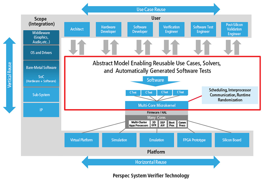
- Perspec System Verifier, a software-driven verification tool that helps engineers define use cases and generate reusable tests. (Use case verification is an important aspect of a shift left methodology).
- Acquisition of Jasper Design Automation, the leading provider of formal analysis tools. This technology will be brought into the Cadence System Development Suite, which includes connected platforms for virtual prototypes, emulation, simulation, and FPGA-based prototypes.
- A new solution for automotive safety verification and compliance to the ISO 26262 safety specification.
- Protium FPGA-based prototyping platform, which is aimed primarily at pre-silicon software development and debugging. It is part of the System Development Suite.
In 2014 Cadence also acquired Forte Design Systems, a pioneer of high-level synthesis, and in February 2015 Cadence rolled out Stratus High-Level Synthesis (HLS), a product that combines HLS technologies from Forte and Cadence. Also in 2014, Cadence strengthened its signoff offerings with the Voltus-Fi Custom Power Integrity Solution and the Quantus QRC Extraction Solution.
Cadence also continued to fill out its extensive design IP and verification IP offerings. Cadence design IP includes memory, analog/mixed-signal, interface protocols, DSPs, and Tensilica® Xtensa processors. Cadence provides IP subsystems for video, audio, image processing, and more.
EONEWS: What are you doing to implement your strategies (partnership/agreement, new acquisitions, investments in activities like R&D, people…)?
Cochran: The main Cadence acquisitions in 2014 are those mentioned above, Forte Design Systems and Jasper Design Automation. Meanwhile, Cadence continues to develop products internally through its extensive and growing R&D teams. The Forte and Jasper acquisitions added key personnel to those teams.
Cadence has deep partnerships with foundries and is engaging in “vertical co-optimization” in order to optimize tools and IP for advanced process nodes such as 16/14nm and 10nm. Like shift left, vertical co-optimization turns a serial process into a parallel process in which steps such as process development, cell libraries, EDA tools, and IP are developed concurrently. One example: in 2014 Cadence announced that its tools and IP enabled the first production TSMC 16nm FinFET SoC.
EONEWS: What are the most important applications?
Cochran: In previous years you could point to a few applications (PCs, tablets, smartphones) that served as primary drivers for EDA. With IoT there will be thousands of potential applications. It’s hard to say what will be most important, given what IoT can bring to automotive, industrial, medical, wireless, and consumer marketplaces. Like the early Internet, the market will sort out the applications that people are actually willing to pay for. An ability to design systems with applications in mind, and get them out the door quickly while keeping costs low, will be critical for success.
Let’s not forget that IoT is not just about devices — it also concerns the cloud infrastructure, which is where most of the data will reside. Thus, EDA vendors must be prepared not only to help designers with low-power, low-cost devices, but also with a new generation of servers that can route and store data quickly with low power consumption.
EONEWS: What are the key factors that set your company apart from the competition?
Cochran: Cadence pays close attention to the needs of its customers and works closely with users on new technology development. Cadence tools are backed by rigorous quality testing, hundreds of R&D engineers and in most cases, many engineer-years of customer experience.
No other EDA vendor offers the full range of solutions that Cadence provides. From custom/analog tools to advanced-node digital implementation, from hardware/software co-development platforms to metric-driven functional verification, from chips and packages to boards and systems, Cadence provides a complete and integrated set of capabilities for today’s most challenging electronic systems. Add the growing Cadence design IP and verification IP portfolios, and you have a complete set of capabilities for SDE as well as the needed prerequisites for a shift left methodology.
EONEWS: And in the middle/long term (if you have a crystal ball)?
Cochran: In the middle term, we see a growing move towards SDE as systems companies become more engaged in both hardware and software design. A shift left methodology will be needed to deal with the massive complexity that’s possible at advanced process nodes, as well as with IoT devices at mature nodes that must be power-efficient and low-cost. Reusable, configurable IP will become more and more crucial, and it must be tightly integrated with design tools. And hardware/software co-development and optimization will be needed to meet time-to-market and quality demands.
EDA may be a “mature” business, but there are a lot of challenges and opportunities ahead. In the long run EDA will encompass far more than it originally did. And EDA will continue to enable the electronics revolution that is shaping our world. It’s a fascinating time to be involved in this crucial industry.
Edite by the the Editorial Staff
Contenuti correlati
-
 Cadence expands Pfizer’s license to molecular design software
Cadence Molecular Sciences (OpenEye)—a business unit of Cadence—announced that Pfizer Inc. has signed an agreement to extend and expand access to Cadence products and programming toolkits for advanced molecular design. “We’re excited to continue to support Pfizer...
Scopri le novità scelte per te
-
Cadence expands Pfizer’s license to molecular design software
Cadence Molecular Sciences (OpenEye)—a business unit of Cadence—announced that Pfizer Inc. has signed an agreement to extend...
News/Analysis read all ▶
-
 Anglia Live expands footprint into Europe
Anglia Components PLC recently announced it is bringing the Anglia Live eCommerce platform to...
-
 Renesas expand its power semiconductor production capacity
Renesas Electronics announced that it has started operations at its Kofu Factory, located in...
-
 VIA optronics and Antolin unveil Sunrise
VIA optronics and Grupo Antolin–Irausa, a global provider of automotive technology solutions, recently unveiled...
Products read all ▶
-
 New rev of MIKROE ’s NECTO multi-architectural IDE
MIKROE has announced that the latest version of its multi-architectural IDE, NECTO Studio 6.1,...
-
 Neousys debuts new IP66 waterproof computer with Intel 13th/12th-Gen Core
Neousys Technology adds a new series to its waterproof industrial computer family featuring an...
-
 TDK-Lambda: new Class I & II industrial 10 to 50W power supplies
The TDK-Lambda ZWS-C series of 10, 15, 30 and 50W rated industrial AC-DC power...

